China has started mass-producing its own machines for printing chips. On 28 July 2026, Reuters identified the builder as Shanghai Aishengna Electronic Technology Group, a little-known state-owned firm putting about five immersion deep-ultraviolet scanners on the floor this year and roughly 20 in 2027, headed to SMIC, Hua Hong Semiconductor and memory-maker CXMT.
This is DUV, not EUV. The tools are aimed at 28 nm and above. They are not ASML-class. Goldman Sachs, in a report dated 24 August 2026, still has China 34% short of advanced-chip self-sufficiency in 2035, with SMIC's advanced-node yield around 23% against TSMC's 90%+.
That is still a real factory, not a lab briefing. The West blocked EUV outright and tightened DUV. Beijing is now building DUV at home.
Why it matters
Lithography is the bottleneck Washington actually closed. ASML of Veldhoven is the only company that sells extreme-ultraviolet scanners — the machines that print the finest circuits in a single pass. The Netherlands, under U.S. pressure, has never licensed an EUV tool to China. ASML told Reuters as much in December 2025: no EUV system has ever been sold to a Chinese customer.
What Chinese fabs could still import, until the latest rounds of controls, were older immersion DUV tools: 193-nanometer argon-fluoride scanners that put a film of water between the lens and the wafer. Those machines make 28 nm chips in one exposure. With extra masks — multi-patterning — they can be pushed toward 7 nm and 5 nm. SMIC has been doing the second half of that trick on an installed ASML fleet since 2022. The new fact is a domestic supplier for the first half.
If the Aishengna tools qualify, Chinese foundries get scanners that a future ban on sales or servicing cannot switch off. That is the point of localization. It is not a leapfrog. It is a supply path for the mature-node iron that still runs most of China's wafer starts, and for the multi-patterning workaround that runs the rest.
The numbers
| Figure | Source | |
|---|---|---|
| Aishengna DUV, 2026 | about 5 tools | The Information, 27 July 2026; Reuters names the firm 28 July |
| Aishengna DUV, 2027 | roughly 20 tools | same |
| ASML immersion DUV, typical year | about 130 systems | Tom's Hardware, 4 Aug 2026 |
| First customers named | SMIC, Hua Hong, CXMT | Reuters / The Information |
| Aishengna registered capital | 7 billion yuan (~$1.0 billion) | Reuters, corporate records, 28 July |
| China share of ASML net sales, H1 2026 | about 16% | Reuters, 28 July |
| SMIC advanced-node yield, 2026 | about 23% | Goldman Sachs via SCMP, 24 Aug 2026 |
| SMIC 5 nm yield | as low as 20% | AEI, 21 April 2026 |
| TSMC yields at comparable nodes | can exceed 90% | Goldman / SCMP |
| China advanced-chip supply gap | 92% of demand in 2025 → 34% in 2035 | Goldman |
| 2035 supply vs demand | 410,000 vs 619,000 wafers/month | Goldman |
Five Chinese tools against roughly 130 Dutch ones is not a market takeover. It is a start. JPMorgan, in a note Reuters quoted that Tuesday, said producing a handful of immersion DUV tools is not high-volume manufacturing, "where yield, overlay, throughput and reliability over thousands of wafer runs are what matter." ASML shares dropped 8% on the Information story; they did not comment, nor did SMIC, Hua Hong, CXMT or Aishengna.
How they got here
Aishengna was set up in August 2023 with two state shareholders: Shanghai Electric Holding and a subsidiary of Shanghai International Trust. It has no public website. Reuters' source said it folded in engineering teams from lithography startup Yuliangsheng — an affiliate of Huawei-backed equipment maker SiCarrier, which had been testing a DUV prototype last year — and from Shanghai Micro Electronics Equipment (SMEE), the long-standing domestic scanner house. Corporate records put Aishengna and Yuliangsheng at the same Shanghai address.
The Information broke the production story on 27 July without naming the firm; Reuters named it the next day. Tom's Hardware (4 August) says the tool prints 28 nm-class features in a single exposure and can be pushed to 7 nm, theoretically 5 nm, by multi-patterning. Reuters did not quote a node. No throughput or overlay figures have been published. Tom's says the first units are for production-line validation, not volume.
That matches how SMIC already makes advanced chips. SemiAnalysis's teardown of Huawei's Kirin 9030, published 14 June 2026, found SMIC's third-generation 7 nm (N+3) at a 32.5 nm minimum metal pitch — TSMC N6-class density, paid for with aggressive DUV multi-patterning. Export controls did not stop the silicon. They made it slower, more expensive, and harder to yield.
The American Enterprise Institute's Lithography Loophole report (Ryan Fedasiuk and Julia Torres, 21 April 2026) put SMIC's 5 nm process at yields as low as 20% and costs 40–50% above TSMC. Goldman used 23% for advanced nodes in 2026 and assumed 50% by 2030 and 75% by 2035 — still without EUV. TSMC, on EUV 7 nm since 2018, can exceed 90%. That gap is the export-control regime, measured. Goldman's 10-year math is still a Chinese ramp: supply growing 46% a year against 17% demand, a 92% hole in 2025 shrinking to 34% in 2035. Even then, 410,000 wafers a month against 619,000 of demand. Full self-sufficiency is not the base case.
What this is not
It is not EUV. A Reuters investigation published 17 December 2025 described a high-security Shenzhen laboratory with a prototype assembled in early 2025 that generates extreme-ultraviolet light but has not produced working chips. The industry wavelength for EUV lithography is 13.5 nm. The government's target is working chips by 2028; people close to the project told Reuters 2030 is more realistic. ASML's own first EUV prototype dates to 2001; commercial chips arrived in 2019. A light source is not a scanner, and a scanner that has never exposed a good wafer is not a product.
It is not a U.S. surpass. ASML still holds the EUV monopoly. China's new DUV line is a handful of mature-node tools, with multi-patterning as an option, against the company that still supplies most of the world's immersion capacity. Localization of a tool class the West tried to ration is a strategic fact. It is not a process-node fact.
What to watch
Three markers, and only three, will tell you whether Aishengna is a factory or a briefing.
- A qualified wafer. Published overlay, throughput and yield from an Aishengna tool at SMIC, Hua Hong or CXMT — not a source saying mass production has begun.
- The 2027 count. Twenty tools is four times this year's plan. If the number lands near 20, the domestic DUV line is real. If it stalls at a handful, it was a prototype with a press cycle.
- An exposed wafer in Shenzhen. Working chips from the EUV prototype before 2028 would change Goldman's arithmetic. Light without a chip does not.
Until then the sourced claim is: Shanghai Aishengna, 28 July 2026, about five immersion DUV scanners this year and roughly 20 next, 28 nm and up, not EUV, not a U.S. surpass.
Sources
- Reuters exclusive, Fanny Potkin, 28 July 2026 — China starts production of home-grown immersion DUV chipmaking tools (full wire text fetched via Global Banking & Finance reprint; reuters.com returned 401 from this fetch)
- Reuters, 27 July 2026 — China begins making homegrown DUV chipmaking tools, The Information reports
- Reuters via Asahi Shimbun, 17–18 Dec 2025 — Shenzhen EUV prototype generates EUV light, no working chips; 2028 target, 2030 more realistic; ASML: no EUV ever sold to China
- AEI, Fedasiuk & Torres, 21 April 2026 — The Lithography Loophole (SMIC 5 nm yields as low as 20%)
- SCMP, Howard Liu, 24 Aug 2026 — Goldman: 34% advanced-chip shortfall in 2035, SMIC yield 23% → 75%
- TechTimes, 24 Aug 2026 — Goldman / AEI yield and self-sufficiency recap
- SemiAnalysis, 14 June 2026 — SMIC N+3 / Kirin 9030 teardown, 32.5 nm metal pitch
- Tom's Hardware, Luke James, 4 Aug 2026 — ~130 ASML immersion/year; 28 nm-class single exposure reported, unconfirmed
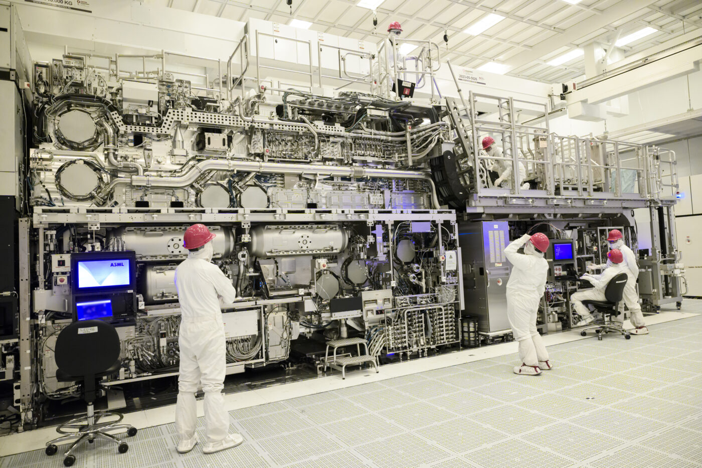
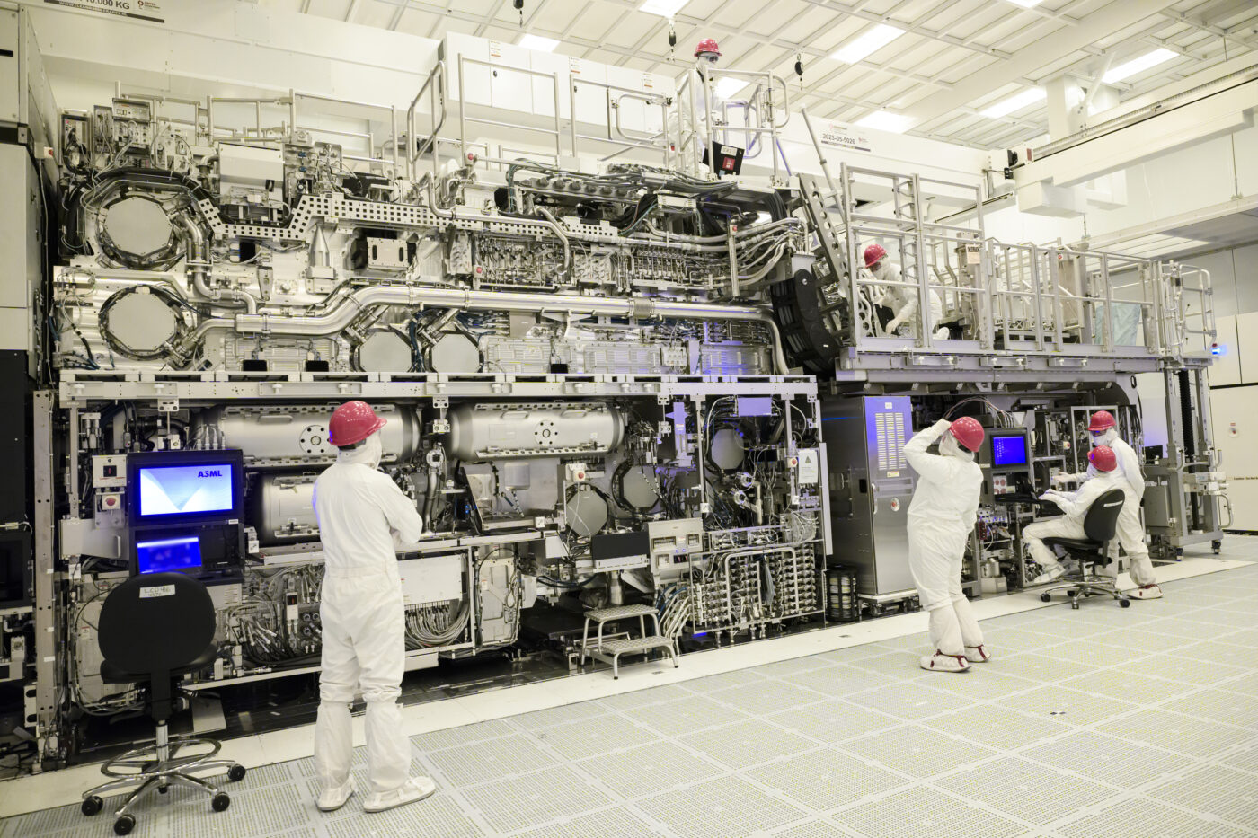
- Cover: Intel Newsroom High-NA EUV press kit — photo, Credit: Intel Corporation